Taiwan Semiconductor Manufacturing Co. today announced plans to invest an additional $100 billion in its U.S. manufacturing facilities.
The investment comes on top of the $65 billion the chipmaker has already committed to building three fabs in Arizona. In a press conference with President Donald Trump, TSMC Chief Executive Officer C. C. Wei said the new investment will help the company produce artificial intelligence processors. It already makes such chips for Nvidia Corp., Advanced Micro Devices Inc. and other market players.
TSMC will use the additional $100 billion investment to build three more fabs in the U.S. Additionally, it plans to open two advanced packaging facilities. Advancing packaging is the circuitry that chipmakers use to combine multiple silicon dies into a single processor. Nvidia’s data center graphics cards, for example, rely on the technology to link their logic circuits with the onboard HBM memory.
The chipmaker’s new investment initiative will also see it establish a stateside research and development center. Its research organization is responsible for designing its chip manufacturing processes. Additionally, it develops new materials and transistor structures designed to boost processor efficiency.
It’s unclear what manufacturing processes will be used by the three new fabs that the company plans to build. TSMC also didn’t specify which advanced packaging technologies it plans to make in the U.S. The company offers several types of packaging that each target different use cases.
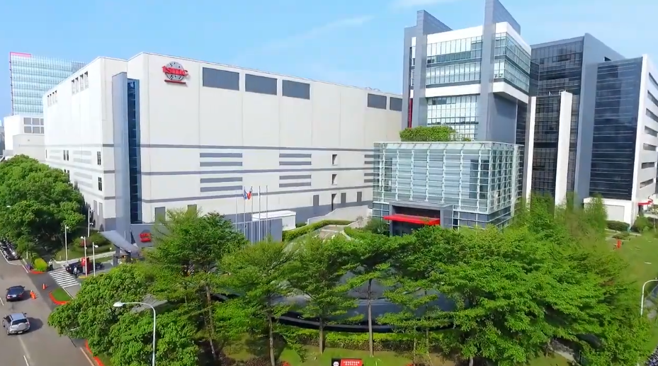
TSMC’s first U.S. fab came online last year. It makes chips based on four-nanometer technology, which is one generation behind the company’s latest three-nanometer processor. The plant is located on a campus in Phoenix, Arizona, where TSMC is also building two other chip plants.
When TSMC announced plans to start making chips in the U.S., it set aside $12 billion for a single Arizona fab. The company upped that number to $40 billion in 2022 with the goal of adding a second plant. Last year, TSMC revised the plan again and announced its intention to build a third fab next to the two other plants. The latter change brought the project’s total price tag to $65 billion.
The third fab that TSMC is building in Arizona will start producing chips by the end of the decade. It’s expected to use the company’s upcoming two-nanometer manufacturing technology, which features a new transistor design known as the gate-all-around architecture. Gate-all-around transistors are easier to customize for specific use cases than current circuits and manage the flow of electricity more efficiently.
With the additional $100 billion commited today, the initiative now ranks as the largest foreign direct investment in U.S. history. The fab expansion is expected to support 40,000 construction jobs over the next four years. Afterwards, TSMC expects to create tens of thousands of tech jobs across its facilities.
Photo: TSMC
Your vote of support is important to us and it helps us keep the content FREE.
One click below supports our mission to provide free, deep, and relevant content.
Join our community on YouTube
Join the community that includes more than 15,000 #CubeAlumni experts, including Amazon.com CEO Andy Jassy, Dell Technologies founder and CEO Michael Dell, Intel CEO Pat Gelsinger, and many more luminaries and experts.
THANK YOU


