Nvidia dominates the global market of chips for artificial intelligence (AI) with a quota that during the last three years has ranged between 80 and 94%, according to FourweekMBA. Your leadership is supported by A very competitive hardware and a software ecosystem in which CUDA (Compute Unified Device Architecture) It has an essential role. This technology brings together the compiler and development tools used by programmers to develop their software for NVIDIA GPUs.
However, the company led by Jensen Huang has a fundamental partner: TSMC. Nvidia designs the chips for AI and this manufacturer of Taiwanese semiconductors, the largest on the planet with a global quota close to 60%, produces them. Its strong leadership is the result of its peak technology and titanic production capacity. TSMC has many important customers, such as AMD, Qualcomm, MediaTek or Broadcom, among many others, but thanks to the AI NVIDIA rise, it has established itself as its second best client only behind Apple.
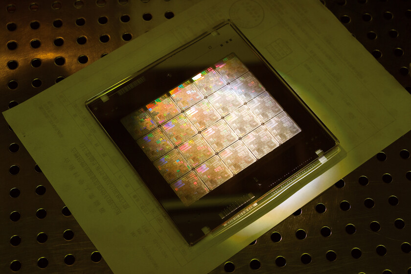
Presumably TSMC is about to start making 2 NM GPU for NVIDIA, but this is not the only thing that this chips manufacturer is going to do for one of its best customers. And this Taiwanese company has decided to launch an expansion plan for five years of its manufacturing capacity of integrated circuits using its advanced packaging technology Cowos (Chip-on-Wafer-on-Substrate). According to Beth Kindig, of the I/O Fund consultant, this technology will monopolize between 50 and 60% of the market in 2025 compared to 15% he held for 2024.
The synergy of these companies is indisputable
The high demand for GPUs for AI with Blackwell MicroAritectura de Nvidia is largely responsible for the implementation of this plan. The company led by Jensen Huang can respond better to the needs of its customers and will see how its competitiveness is increased in a phase in which Depseek and other Chinese companies represent a challenge. In March 2024 TSMC he officially announced that he was building two cowos packaging plants in the town of Chiayi, housed in southern Taiwan.
However, this is not all. He also shuffled the option to put a plant more specialized in this advanced packaging technology in Japan, presumably on the island of Kyushu, in which this company is currently building two production plants of avant -garde semiconductors. In any case, there is something else. And it is that Chiayi plants will be trained to work, in addition to the packaging cowos, With advanced Info and Soic technologies (System on Integrated Chips).
Nvidia and TSMC synergy is indisputable, but this recipe requires a third ingredient: SK Hynix
It is evident that TSMC wants to cover your back well and look to the future to prevent its production capacity from being threatened by a bottleneck. An interesting note: currently the Cowos packaging is being used with the AMD Instinct Mi250 chips and with the A100, H100, H200, B100 and B200 NVIDIA GPUs, as well as in its derivatives. The review used in these last two chips, the B100 and B200, is known as Cowos-L. Before the TSMC ends this year, you will be able to process no less than 60,000 wafers per month using its advanced packaging technology.
The synergy of Nvidia and TSMC is indisputable, but this recipe requires a third ingredient: SK Hynix. This South Korean manufacturer of memory chips leads the HBM memories market (High Bandwidth Memory) that work side by side with the GPUs for ia with a shocking authority. Its market share touches 70%, so that the remaining 30% are distributed by Samsung and Micron Technology. After them, Chinese manufacturers of Yangtze Memory Technologies Co. (YMTC) and CXMT (Changxin Memory Technologies).
At the end of 2024 SK Hynix took advantage of the celebration of an innovation forum organized by TSMC to publicize its mastery of the manufacture of HBM memories. According to SK Hynix itself, its MR-MUF process, which, in broad strokes, is a technology that makes possible a faster punch of the dram compared to the TC-NCF process that other companies use, it has allowed it to achieve an efficiency 8.8 times higher than that of Samsung and Micron. This simply means that it manufactures its HBM chips much faster than its main competitors.
SK Hynix is manufacturing 12 -layer HBM3E memories on a large scale while Samsung and Micron have problems with their production
As we can intuit, the speed at which a company that is dedicated to manufacturing semiconductors is capable of producing its integrated circuits deeply condition its competitiveness. It is evident that greater efficiency will allow you supply more guarantees to your customersespecially in an upward market like that of HBM memories. In addition, SK Hynix is manufacturing 12 -layer HBM3E memories on a large scale while Samsung and Micron have problems with their production. In any case, both Samsung and SK Hynix are already working on the development of HBM4 memories with the purpose of catapulting their competitiveness.
Here it is precisely where Nvidia appears. SK Hynix announced in October 2024 that he intended to deliver the first HBM4 memory chips to his clients during the second half of 2025. However, Jensen Huang asked him to advance the delivery. It was confirmed by Chey Tae-Won, the president of SK Group, so it is absolutely reliable information. Why does NVIDIA require so urgently the HBM4 chips? Simply because you need to support your chips for the most capable with the most available energy and energy efficiency memories. And in this field SK Hynix currently has the pan well grabbed by the handle.
Imagen | TSMC
In WorldOfSoftware | South Korea fears US reprisals. To avoid their old lithography equipment, they take dust on a warehouse


