
Faced with an American embargo which deprives him of the equipment of lithography EUV (the ultra-precise engraving process) the most advanced, the Chinese giant has decided to change the playing field.
During the IEEE symposium in Shanghai on May 25, 2026, He Tingbo, president of the company’s semiconductor division, formalized a bold strategy.
Huawei has unveiled its Tau’s Law (τ Scaling Law), a new principle of chip design, and the architecture LogicFolding. It is no longer a question of running madly after miniaturization at all costs, but to invent a new path.
The goal is to achieve a transistor density equivalent to a 1.4 nanometer process by 2031, which would be a real snub to the arsenal of American restrictions imposed since 2019.
What is this new approach called “Tau’s Law” and “LogicFolding”?
The Law of Tau is a new guiding principle proposed by Huawei to guide the development of chips, replacing the famous Moore’s Law.
Instead of just focusing on reducing the size of transistors, it aims to reduce the signal propagation time (the famous Tau, τ). To achieve this, Huawei has developed the architecture LogicFoldingwhich consists of “folding” the logic of the chip on two layers instead of just one.
This 3D structure allows drastically shorten the wires inside the chip, thereby increasing density and energy efficiency. It’s an architectural sleight of hand: if we can’t engrave finer, we’ll build smarter.
According to He Tingbo, this approach has already made it possible to design and produce 381 different chips over the past six years, proving its validity on a large scale.
How does this strategy defy the famous Moore’s Law?
Moore’s Law, a historic observation formulated by Gordon Moore, postulated that the number of transistors on a chip doubled approximately every two years. However, this law today comes up against physical and economic limits colossal.
Huawei’s Law of Tau offers an alternative: it replaces “geometric scaling” with ” temporal scaling “. The goal is no longer just to cram more transistors together, but to ensure that information flows faster between them.
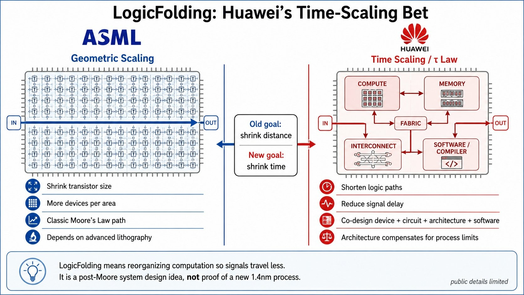

This is a radical change in philosophy. Rather than depending on a single advance in manufacturing processes, Tau’s Law advocates a optimisation collaborative at all levels: circuit design, packaging, software and systems.
Jensen Huang, CEO of Nvidia, himself admitted that Moore’s Law was “dead”. Huawei provides here a concrete proposal for the future, an alternative path for the technology industry. semiconductorseven if, of course, this does not resolve the fundamental limits of matter approached little by little.
What are the concrete applications and ambitions of Huawei?
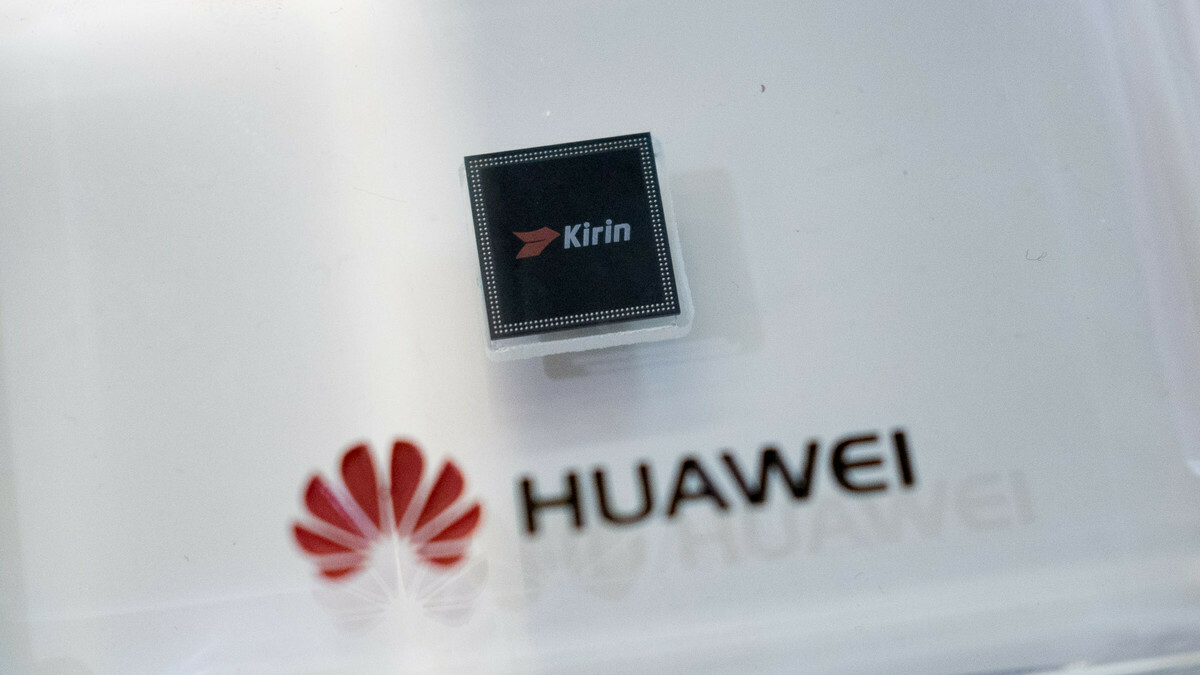
The first show of force is imminent. Huawei announced that its next puce Kirindesigned to equip smartphones in the series Mate 90 in fall 2026, will be the first to fully integrate the architecture LogicFolding.
This announcement is also that of a reconquest of the high-end market against Apple. But the ambition is much broader: Huawei projects that this technology will make it possible to achieve a density equivalent to 1.4 nanometer process by 2031.


Huawei Mate 80
Such a goal would put China on a par with global leaders like TSMC and Intel, but via a completely different path. The real test, however, will be scaling up: applying this technology to chips dedicated to artificial intelligence in data centers.
This is where Huawei’s bet will be validated or not, and where we will see if this ingenuity can really compensate for access to Western technologies.
Is this strategy really viable or is it just a hype effect?
If the promise is tempting, experts call for caution. Paul Triolo, an analyst at DGA Group, points out that bending logic circuits can increase density, but doesn’t magically solve all problems.
THE heat challenges (thermal stresses), to the energy consumption and to manufacturing yields (the percentage of functional chips) are immense with such complexity of packaging (assembly of the chip).
This approach is more of a “systems-level optimization doctrine” than a true revolution in fundamental manufacturing. The Achilles heel of this strategy may be its ability to be mass-produced reliably and cost-effectively.
The success of the Kirin chip will be a first indicator but the battle for AI chips will be the final judge. The ingenuity is there, but execution on a very large scale is an equation that remains to be solved for the Chinese technological ecosystem.