Integrated 2 Nm circuits will disembark in the market in style for 2025. Users know that nanometers have lost much of their usefulness, and that, in reality, They represent a category of semiconductors. In fact, they no longer faithfully reflect the length of logical doors or other physical parameter, such as the distance between transistors. However, the very rapid development of the chips reminds us that every step we take place a little closer to the physical limit of silicon technology, although, in reality, this challenge is not new.
The main manufacturers of integrated circuits and numerous research groups linked to some of the most important universities on the planet have been working on a solution to this challenge. Decades, even. There are currently several open research lines, and possibly the solution will require betting on one of them, but it is even more likely that the way to follow invites us to allow several of the proposals to be working on.
The first 2D computer in the world is here
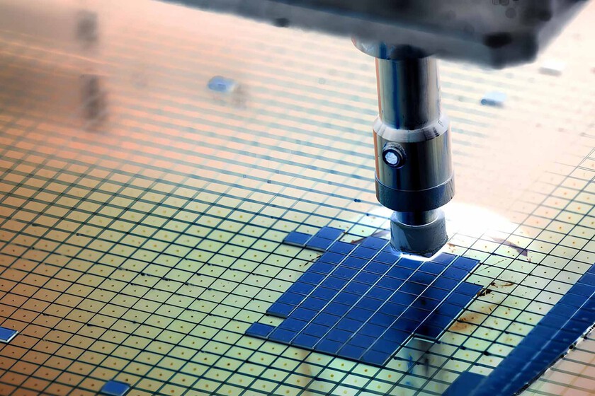
A team of researchers from the University of Pennsylvania (USA) has published in Nature an interesting article in which he explains the procedure that has followed to manufacture the first functional CMOS processor using two -dimensional materials (2D) of a single thick atom. The really revolutionary thing is that they have used molybdenum disulfide and tungsten dyslelenex with the purpose of producing more than 2,000 transistors capable of executing logical operations. They have not used a single silicon atom.
“We have first demonstrated a CMOS processor built completely with 2D materials”
However, it is also important that we do not overlook that the materials they have used, which, as I have mentioned, have only one thick atom, maintain their properties at that scaleunlike silicon. The leader of this project, Professor Saptarshi DAS, said that “silicon has promoted notable advances in electronics for decades by allowing continuous miniaturization of field effect transistors (FET or Field-Effect Transistors)”.
“However, as silicon devices miniaturize their performance begins to degrade. 2D materials, on the other hand, maintain exceptional electronic properties at the atomic level, placing a promising path before us,” explains Das. “We have demonstrated for the first time a CMOS processor built completely with 2D materials combining molybdenum disulfide transistors and tungsten tungsten dysleeniuro cultivated in large areas.”
All this sounds very good, but there is no doubt that for users the most relevant is to know what impact this technology will have in our experience if it becomes popular. “Our 2D CMOS processor operates with low power voltages, Minimum energy consumption And it can execute simple logical operations at frequencies of up to 25 kHz, “said Ghosh, one of those responsible for the project. This is the heart of the matter.
We are only at the dawn of the technology known beyond silicon, but presumably the chips with molybdenum disulfide transistors and tungsten dislendiuro will allow the manufacture of much faster and more compact computers than the current ones, as well as perceptibly more efficient from an energy point of view.
More information | Nature
In WorldOfSoftware | Intel and TSMC lead the revolution of photonic chips. His problem is that China has just done fully in this war


